How to DIY an Open USB FXS dongle
About this page
This page is all about how to assemble your own DIY board. It contains all the information you need in order to assemble and test an Open USB FXS board with your own bare hands (OK, and a few basic electronics tools).
Inventory
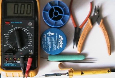
First, let us review the absolutely necessary tools and materials required to assemble a board on your own. Of course, if you own a reflow oven, a laser beam soldering facility, a pick-n-place machine and a stencil printer, you are doing far better, but this page will describe how to build a board with tools readily available to (or cheap enough to) the average electronics hobbyist. The absolutely necessary tools are, then:
-
A soldering iron. Mine is a 17W Antex. It needs to have a fine tip.
-
A pair of twizzers.
-
A holding tool and a cutter.
- A Volt/Ohm meter (preferrably with a beeping contact test function).
-
Solder (60/40) and soldering paste/flux.
The following are also needed but not shown in the picture:
-
A magnifying glass.
-
Solder-removing wire (“thread”).
- Pure alcohol and brush, cloth or cotton pads for cleaning.
- A thin steel sewing needle and some toothpicks for cleaning.
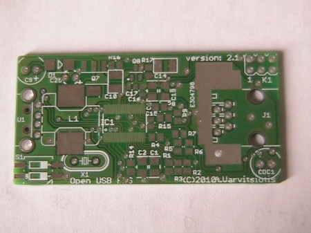
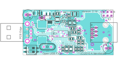
Before starting anything else, let us review your board. This is the top view of an Open USB FXS PCB:
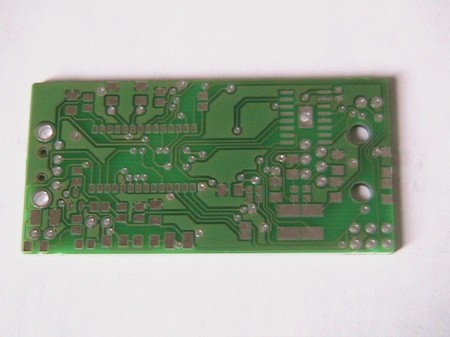
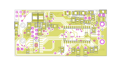
, and the bottom view is on the next picture. Unfortunately, the bottom side does not have a silkscreen (it would be more expensive).
You will also need four pages of paper (preferrably printed, I like to have them handy): two printouts of the top and bottom sides of the boards with component names and placements, and the two pages of the BOM. Here they are (download here for the top and here for the bottom views):
Top view:
Bottom view:
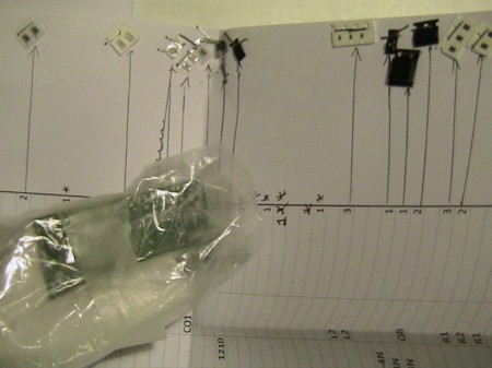
The BOM printout will be included in your DIY package, with the appropriate SMT components stapled next to each component’s name. Bulky or easy-to-identify components will come loose (not stapled to the printout). Here is an example of how the DIY kit will look like when unpacked (I know stapling the components may look not too elegant, but believe me, it’s very convenient). The plastic bag contains the non-stapled components, marked with *.
Here is a link to the BOM, and here is an excerpt showing what it looks like:
Note in particular the two rightmost columns, “Same as” and “Pieces per board”. In order to make packaging easier, all components with the same value will be stapled in the first row with that value, so in subsequent occurrences of the same value you should follow the “Same as” reference to find the component.
Please note that components marked with a ‘=’ sign are not part of the BOM and they are not included in your DIY kit. These components are for an alternative design using a 150uH inductor. Also note that there is an on-PCB jumper that is not a physical component. Finally, the 6-pin pinhead connector K1 is not included in the DIY kit, since this is only required in order to do the initial programming of the PIC 18F2550 chip. The chip will come pre-programmed in your DIY kit, so K1 is not needed.
It goes without saying that you should verify your kit and make sure that all required materials are included. What if something is missing? Well, before mailing me, please try to look a second time. If is still missing, please contact me.
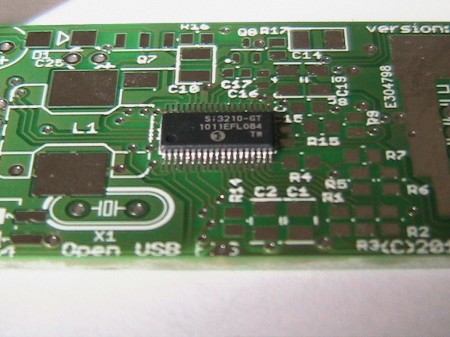
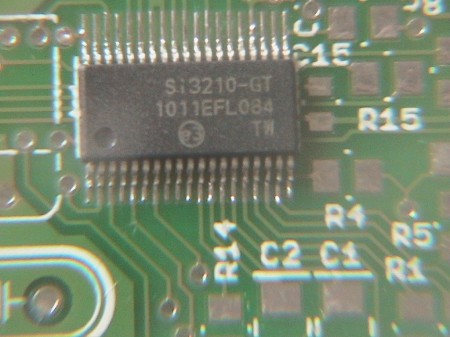
First step: soldering the Si3210
Ok, now that you have run an inventory, it’s time to begin. The very first step is also probably the hardest one: solder the hair-thin pins of the Si3210 (IC1). Before you begin, make sure that you and your working environment are ESD-free (e.g. grounded), since all three ICs are sensitive to ESD. Same goes for your soldering iron, which should be grounded — via the mains supply or otherwise.
My method for soldering the 3210 is one I have tried quite a few times and gave me the best results compared to others. In order to follow this method, do the following (please read all steps first):
-
Apply soldering paste/flux to the tiny-thin pads of the Si3210 and then heat up with the soldering iron slightly tinned with solder. Try to leave a moderate amount of solder on each pad. If a small “droplet” is formed, make sure this droplet goes to the outward side of the pad (i.e., it is not facing the opposite-side pad). Remove any excessive solder or short-circuits with the solder remover and soldering paste. Make sure not to heat the PCB pads for too long, because doing so will make them detach from the board, thus causing irrepairable damage to your kit. You may just as well pass the soldering iron over all the pads, thus leaving only a small amount of solder on each pad (if you do that, don’t pass the iron too fast, or else the amount of solder will not be sufficient).
-
Clean thouroughly the area on and around the pads with alcohol and make sure there is no remnant soldering paste/flux. Failure to clean the area will most probably leave spots of paste or flux between the pins of the 3210 with low impedance at high frequencies, and this will cause your board to fail or misbehave. Sweep out any alcohol remainders, too, before you proceed.
-
From that step on, use the magnifying glass. Put the Si3210 in place. Mind the correct placement of the chip. Because of the tiny solidified solder drops on the pads, the chip will tend to slip forwards or backwards — that’s OK. The pads are long enough on purpose (in order to “store” as much solder as needed), so try to leave an equal length of the pads free on each side of the chip. Make sure the chip is correctly in place (use the magnifying glass if needed), and hold it there with your left thumb (assuming you work best with your right hand, or vice versa otherwise).
-
As you are holding the board with the chip on it, heat shortly with the soldering iron the tiny solder drop on the bottom right pad, pushing it towards pin 19 of the chip. Solder should cover the pin. Now the chip stays in place, but it is free to revolve around its pin #19 (so be careful not let it move too much, or else you risk breaking the pin).
Do not worry at this time if you have soldered pin #18 together with pin #19 . -
Turn the board 180 degrees around. Without letting or forcing the chip to move too much, adjust its position, making sure that the pins are as much as possible aligned with the underying pads. Then, still holding the chip with your left thumb, heat the solder drop on pad #38. The chip should now be soldered almost firmly in place. Make sure it is indeed soldered firmly (try pushing it gently).
Do not worry at this time if you have soldered pin 37 together with pin 38. -
Before proceeding, examine closely the pins of the chip with the magnifying glass. If there are any individual pins gone wry, use the sewing needle to place them back, so that they are exactly over the corresponding pad. On the contrary, if all pins on one side are mis-aligned, do not try to fix this by bending the pins; instead, re-heat one of the two soldered corner pins. Make sure that the two soldered corner pins (#19 and #38) have not moved too close to their neighboring pins. If they have, heat up again the pad (briefly!) while using the sewing needle to bend the soldered pins back into proper distance from their neighbors. When finishing with these slight corrections, the chip should be exactly in place, and no pin should be closer than others to its neighbors.
-
One by one, solder all other pins, using this method: heat up the solidified solder drop on the pad and push it towards the respective chip’s pin. Then exercise some light pressure with the tip of the soldering iron to push the pin towards the pad, and instantly remove the soldering iron.
-
Remove any shorts using the solder remover thread. It’s best to apply a moderate amount of soldering paste or flux onto the thread (not on the pins of the chip or the short itself though, unless you cannot remove the short otherwise).
-
Clean up again the area with alcohol. Examine visually the results with the magnifying glass, trying to spot any solder drops or paste remnants between the pins or the pads. Use the sewing needle to remove any such, avoiding to re-heat any pins unless it is necessary.
-
Use the sewing needle to gently push pins back and forth (“back and forth” is not “in and out”, nor “up and down”), thus making sure they are not left unsoldered. If a pin is loose and moves about, make sure to bend it back into place with the needle and then try to re-solder it.
-
Test for both conductivity and short circuits on all pins, using the beeping contact meter.
-
Take a deep breath, then go for a short walk. You ‘ve done it! (If at this stage you have damaged the chip or the PCB, it’s also best to take a walk before you start over with that second DIY prototype you have ordered just in case; after coming back from that walk, use the damaged chip and/or PCB for practicing in order to perfect your skills).
Of course, every person has his/her own preferences and style, especially when it comes to the black art of delicate soldering. If you prefer your own method, feel free to take note of my suggestions and then use your method. Especially soldering with paste/flux should make things easier, however I am not sure how well one can clean the area underneath the chip after that, and paste/flux remnants are almost guaranteed to make the thing fail — this is why I have used this “dry” method, where no paste is applied during final soldering.
Second step: soldering the Si3201
This is a hard one, too, but not as hard as the 3210. While the risks in soldering the 3210 are mostly in mis-aligning the pins, leaving pins un-soldered, or creating shorts, the risk with the 3201 is overheating rather than anything else. This is so because of the thermal pad underneath the chip. So, here is my suggested method for soldering the chip.
-
Turn the board so as to work on the bottom side (the one that’s not silk-screened).
-
Do not apply solder to the pads of the chip. Instead, only apply (some paste/flux and) solder to the thermal pad on the PCB. Try not to leave too much solder on the pad, or else the chip will teeter on the solid drop left on the pad. If you do leave too much solder, remove some with the remover thread.
-
Repeat, this time applying a small quantity of solder on the thermal pad of the chip. Same goes here for not leaving too much solder on the thermal and removing excess quantities with the thread.
-
Clean up thouroughly the area on the PCB and underneath the chip from soldering paste/flux remnants.
-
Put and hold the chip into place (mind the correct placement). Use the left thumb for holding the chip. Don’t worry if the amount of solder on the thermal pad underneath the chip (either the PCB or on the chip’s own pad) prevents the chip from sitting correctly on the PCB. This is perfectly OK: excess solder will be flattened during reheating (see the next steps). Just make sure the pins on one of the two sides all make contact with the PCB pads.
-
Solder all the pins on the side that makes good contact to the respective pads. Only solder the pins on one side of the chip, or else you won’t be able to check if the thermal has been correctly soldered (see the next steps). Of course, you should check the alignment of the pins on both sides as you proceed. The chip should now be slightly “lifted” on its one side (the soldered one — see photo below).
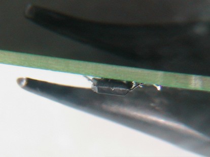
-
Using your fingernail or the needle to pull gently the chip up (the chip, not its pins), make sure you can see the unsoldered side of the chip moving slightly up and down as you are pulling it away from the board and letting it back. Don’t put in too much force or else you risk detaching the soldered pads from the PCB.
-
Turn the board upside-down again, so as to work on the top side. Spot the large hole that gives access to the 3201’s thermal pad for soldering. Heating the solder, leave a moderate amount of it within the hole and then allow one minute to let things cool down. It’s best not to fill up the hole with solder — the more solder you place, the longer you ‘ll have to re-heat.
-
Now place the board with the 3201 facing downwards on a flat surface to serve as a heat sink (e.g., the bottom of a frying pan, or the surface of a metal tool). Heat the solder you have placed on the hole in the previous step, at the same time pressing moderately the board downwards. Stop heating after two-three seconds (while still exercising some pressure downwards). After another two-three seconds, lift the board, let it cool and examine the chip’s position: it should now sit flatly on the PCB, since heating and pressing has now flattened the solder on the thermals. Repeat the pull-the-chip-up-with-your-fingernail test. If the chip’s thermal is correctly soldered to its pad, you will not be able to move the chip as you did before. If the chip is still slack, this means you have to repeat this step. Allow plenty of time between successive attempts so as to let the chip cool down.
-
After the thermal is soldered, do solder also the opposite side of the pins that you had left unsoldered. Remove any excess solder, shorts, etc. and clean up the area thoroughly with alcohol.
Go for another walk. It was hard but you made it. Other components are not as hard as these two chips. Whenever you feel like going on, start with the rest of the assembly.
Soldering the 603 SMT components
Now it’s time to solder all the 603 SMT components, namely C15, C16, C17, C24, C30 and L2, L3 and L4. What makes it hard is their tiny size. But you ‘ll make it. Start from L3 and L4 where space is ample, then move on to the other components. My own method of soldering simple SMT components is as follows.
First, apply a small droplet of solder to one of the component’s pads. Pick the component with the twizers and place it almost in its position, a bit towards the pad that does not have any solder on it. Heat up the pad with the solder, at the same time pushing slightly the component with the tweezers in place. Let it cool, then make sure the component is well in place — if not, make the necessary corrections. Solder the second pad, then “revise” the first pad in order to e.g. remove excess solder.
The same method more or less applies to all SMT components besides 603 ones.
Soldering the PIC
Nothing difficult here. If you have soldered SMT components before, it’s not going to give you a hard time at all.
Don’t forget to solder the pads of JLVP, creating a short-circuit. Failure to do this will cause your board to reset. The jumper is there in case you have a PIC that is configured (“fused”) to disable LVP (low-voltage programming). The PIC chip included with the DIY kit does not have this fuse setting and thus requires the jumper to be short-circuited (see my blog post “A board to be held tenderly” for details).
Move on with SMT components
Solder all SMT components, leaving the bulky ones (inductor L1 and switch S1/S2) for the end. Place Q7 as much as possible towards the edge of the board, to leave enough space for accessing L1’s pads. Do also mind the correct polarity of D1.
Don’t worry about the resistor RDTX on the bottom side missing from your kit (and the BOM). It’s not required and it’s not included in the kit.
The side-view LED LD1 is a bit harder to solder than other SMT components, but it’s not really too much difficult. Mind its correct polarity though.
L1 requires some more attention. Before soldering, you should apply a small amount of solder to both the pads on the PCB and to those of L1 (remove excessive solder with the thread). Then you should hold L1 into place, heat the pads and press L1 towards the PCB. It’s not very hard. Make sure not to leave too much solder on L1’s pad next to the crystal, or else the crystal won’t sit well in place.
Finally…
After finishing with the SMT components, you should make a thorough visual review of the board, as well as test it with the meter to make sure all components are soldered and no shorts exist.
After that, you can mount the trhough-hole components. Start by the crystal, then move on to the capacitors. Pay attention to the polarity of two electrolytic and the one tantalum caps. Finally, mount the RJ11 and the USB plugs.
That’s it, you are done! Clean out once more all flux or paste from your board with alcohol, check once more your board visually, and then move on to the setup and debugging guide page.

September 11, 2010 at 3:49 am
Wow! Great work. That takes a steady hand and good eyesite to pull off. Thanks for the post.
September 11, 2010 at 1:48 pm
Hi Jeff,
Thanks for your comment! Well, I am 45 years old and my sight is not as strong as it used to be, so I wouldn’t be able to do this without a good magnifying glass. And my only secret to keep my hands from trembling was that I never worked early in the morning after late-night drinking :-).
Cheers,
Angelos
August 16, 2011 at 12:55 am
Can I put a standard telephone (aka POTS) to the FSX and call the phone from an apllication to produce a ring? If my pc has 8 usb ports can I connect 8 simple telephones (with 8 controllers) and have an interconnection or call someone in the outside world with VoIP?
I quit drinking around about 12 years and I can have a steady hands but I don’t have the money or the time to make anything although I own the same yellow antex solder as you in the picture which is 24 years old and working! 🙂
Maybe one day at the retirement age I would make a laboratory to do some research.
Greetings from greece.
August 16, 2011 at 6:09 am
Hi Stsoli,
Your greetings from Greece came over to Greece (I am Greek, too :-)). It seems that Antex have made good sales around here, right?
To answer your questions: yes, at least in theory, you can attach eight Open USB FXS dongles to one PC, connect a plain old telephone device to each of them, and have the phones communicate (place calls) among them and/or to the outer world (the latter over VoIP, e.g., over a SIP trunk). I am saying “in theory” because I have not tried that many Open USB FXS devices in parallel and I don’t know how they will perform. From a purely technical standpoint, and although I hate recommending against my own hardware, the right solution for this type of application is a USB FXS “bank”, like the ones Xorcom produces. But you may try a number of FXS boards in parallel as well and see how they will perform. If you don’t have the time to assemble them, you can always have someone else do that for you. I ‘ll contact you in private for more details.
Cheers,
Angelos
February 12, 2012 at 11:53 pm
Hi!
Could you please tell me what do you mean by “you can attach eight Open USB FXS dongles to one PC” – does it mean connecting all of them in parallel, to the same USB port (8:1) or connect as 1:1 (one FXS -> one usb port)?
Thank you
Eugene
February 14, 2012 at 6:48 am
Hi Eugene,
Thanks for your question. My phrase is actually a reply to a former question,
whether one can connect one Open USB FXS on each of the eight ports of a PC.
So, my original phrase is about connecting each dongle to a separate PC port.
In theory, you could also add a USB hub and connect all dongles to a single
PC port via the hub, but I have not tried this configuration and do not know
how well it will perform.
Although my next question to you may be against my “interests” in Open USB FXS,
if I may ask, what would you need eight dongles for? There are other solutions
for such configurations, namely FXS port banks with a single USB interface.
I agree these tend to be more expensive, but technically speaking, they are
sort of a more correct solution for connecting a large number of FXS ports to
an Asterisk PC.
Cheers,
Angelos
November 1, 2012 at 11:22 pm
Is anyone still working on this? Would anyone be willing to sell me a board, preferably completed?
November 14, 2012 at 7:16 am
Hi Jeff,
Thank you for your interest in obtaining an Open USB FXS board!
Usually I do not let comments asking for boards through and instead I reply via email to the email address given in the comment. However it seems that some of the people who post comments don’t look at their supplied email-address mailbox afterwards, so I decided to let your comment through.
The correct way to address inquiries about boards is by mailing me directly to my email address avarvit -at- gmail (dot) com. The usual reply, if I have any boards left (which I think I do right now), is that I prefer, instead of selling Open USB FXS boards, to trade them with other “interesting items” that my “customers” (in this case, you), would like to exchange for a board. This is not obligatory, and you still have the option to pay using money. For details, you should contact me on my email address above.
Cheers,
Angelos
May 11, 2013 at 6:58 am
Hello
Are there any oss software drivers for this device?
Does it work with Asterix? If so which software module?
Does it work with Freeswitch? If so which software module?
Does it work with OpenPBX? If so which software module?
Thanks
g
May 11, 2013 at 4:31 pm
Hi Geofreey,
Thank you for your comment. Open USB FXS has an open-source driver, oufxs, which compiles against Dahdi (versions 2.2 — 2.5 inclusive — 2.6 compatibility is in the oven and should be coming out soon).
In plain English, this means that Open USB FXS is readily compatible with Asterisk.
Just to be able to tell about OpenPBX, please refer me to the exact web page of the project you mean.
Freeswitch claim (http://wiki.freeswitch.org/wiki/OpenZap_Dahdi) that they can interoperate with Dahdi drivers, so Open USB FXS should interwork with Freeswitch, fingers crossed (never tested this; I am just saying “it should”, not “it will”).
Cheers,
Angelos